Special lectures
1 2 3
4 5 6
7 8 9
10 11 12
13 14 15
16 17 18
19 20 21
22 23 24
25
CHARGE-TRANSFER EXCITON TRAPPING AT VACANCIES IN MOLECULAR
CRYSTALS: PHOTOCONDUCTIVITY QUENCHING, OPTICAL DAMAGE, AND
DETONATION
R. W. MUNN and D. TSIAOUSIS
Department of Chemistry, UMIST, Manchester M60 1QD, United
Kingdom
Charge-transfer (CT) excitons constructed from neighbouring
molecular anion–cation or electron–hole pairs are obvious
precursors to photoconduction. They also appear to be implicated
in optical damage, where a mechanism involving multi-photon
ionization has been invoked, and in detonation, where a recent
mechanism proposes CT exciton formation as a more plausible
alternative to the on-site ”local metallization” suggested
previously. The Coulomb attraction between the electron and hole
in a CT exciton is screened by polarization of the crystal, which
therefore helps them to stay apart. However, vacancies remove
polarizable material, so reducing the screening and increasing
the attraction. Hence vacancies constitute traps for CT excitons.
This trapping facilitates geminate recombination, which quenches
photoconductivity. It also releases energy that is available to
distort the lattice further, leading to more trapping, and
eventually to optical damage. Alternatively, the energy released
at such ”hot spots” may initiate chemical reaction leading to
explosive decomposition, i.e. detonation.
Calculations are reported that confirm the existence of CT
exciton trapping near vacancies and quantify the trap depths in
three systems:
- anthracene (where photoconductivity has been extensively
studied);
- acetanilide (where optical damage has been extensively
studied);
- RDX (where detonation has been extensively studied).
Materials for Polymer Electronics Applications –
Semiconducting Polymer thin Films and Nanoparticles
Ullrich Scherf , Polymerchemie, Universität Potsdam,
Karl-Liebknecht-Str. 24/25, Haus 25, D-14476 Golm, Germany, e.mail:
scherf@rz.uni-potsdam.de
The development of organic, semi-conducting polymer-based
light emitting diodes (PLEDs) has demonstrated the enormous
potential of this class of macromolecular materials. Besides
PLEDs also organic materials-based field effect transistors
(OFETs), solid state lasers, photodiodes, and solar cells came
into the focus of scientific and industrial interest, especially
for a future ”all-polymer electronics”.
The lecture reports novel promising results from our polymer
chemistry group in Potsdam related to the synthesis,
characterization and application of para-phenylene- and
polythiophene-type polymers, as well as novel
conjugated/conjugated block copolymers. Some of the materials are
characterized by very high structural regularity, low defect
concentrations, high charge carrier mobility, and exceptionally
good photo- and electroluminescent properties.
Solid layers of semiconducting polymers have been successfully
included as active layers into various electrical and
electro-optical devices. While in most of these cases film
preparation has been performed from solutions of the active
components in organic solvents, the deposition from aqueous
systems would be also desirable. We could now demonstrate film
formation from semiconducting polymer nanoparticle (SPN)
dispersions, which have been prepared in a miniemulsion process.
The particle size of these nanospheres could be controlled in the
range of 50-200 nm. Homogeneous layers could be prepared by spin
coating the dispersions onto suitable substrates. Absorption and
photoluminescence spectra of these novel layers showed no
difference in relation to solution processed films indicating
that the electronic structure of the polymer remains unchanged
upon particle formation.
We propose that the concept of semiconducting polymer
nanoparticles will allow to form multilayer structures by e.g.
depositing a first layer from a solution of a polymer and
overcoat it by semiconducting polymer nanospheres of a second
polymer, followed by e.g. annealing. Most important, this will
allow the formation of a multilayer structure from polymers,
which are highly soluble in organic solvents, without introducing
any additional chemical conversion steps.
OPTICAL GRATING RECORDING IN HIGHLY ORGANIZED THIN FILMS OF
DISPERSE RED 1
A. MINIEWICZ a, M. SOLYGA a, H.
TAUNAUMANG b, M.O. TIJA b
a Institute of Physical and Theoretical Chemistry,
Wroclaw University of Technology, 50-370 Wroclaw, Poland, e-mail:
miniewicz@kchf.ch.pwr.wroc.pl
b Department of Physics, Institut Teknologi
Bandung, Jalan Ganesa no.10 Bandung 40132, Indonesia
Optical grating recording of micrometric dimensions which can
handle gray-levels patterns is investigated in photochromic
material made of Disperse Red 1 (DR1,
4-[N-ethyl-N-(2-hydroxyethyl)]amino-4’-nitro-azobenzene)
molecules vacuum deposited on glass substrate. The properties of
polymers containing DR1 have received enormous attention as they
are suitable for applications such as holographic optical
elements or data storage media. Up to our knowledge thin films of
DR1 have never been investigated before in that respect, except
our recent work [1]. Thin films of DR1 were prepared by vacuum
deposition [2] and have thickness of 0.1 m.
Holographic gratings of periods
within the range of 0.6 m - 12 m were recorded by 514.5 nm light from cw
Ar+ laser using degenerate two-wave mixing technique.
Despite the very small recording layer thickness the diffraction
efficiency measured within a Raman-Nath scattering regime reached
3.5 %. We established, using a grating translation technique [3],
that the light scattering was mostly due to presence of periodic
absorption changes (i.e. amplitude grating).
We studied kinetics of grating recording in function of
incident light intensity and analyzed it using Fourier
transforms. Grating profiles were analyzed in relation to
exposure conditions and in correlation with molecular
organization. Polarizing microscopic studies revealed the
presence of light induced optical anisotropy. Following that we
have checked that polarization sensitive recording is also
possible in this medium. This discovery is a challenging one as
it requires development of a model for grating build-up process
in the DR1 films. We believe that this process is connected with
local heat induced pre-melting then molecular rearrangement
(reorientation in optical field) followed by layer
re-crystallization.
[1] H. Taunaumang, M. Solyga, M.O. Tija, A. Miniewicz, On the
efficient mixed amplitude and phase grating recording in vacuum
deposited Disperse Red 1, in preparation
[2] H. Taunaumang, Herman, M.O. Tija, Optical Materials, 18
(2001) 343.
[3] K. Sutter, P. Gunter, J. Opt. Soc. Am. B. 7 (1990) 2274.
PHOTONIC ENGINEERING OF MOLECULAR MATERIALS
FRANÇOIS KAJZAR
Commissariat à l’Energie Atomique
DRT – LIST, DECS/SEMM/LCO
CEA/Saclay, 91191 Gif sur Yvette, France
The observed recently fast development of photonics, comprised
as science and technology connected with handling of photons, can
be compared to what electronics has known in the last centaury.
This is not only due to the immense development and large needs
for information processing, transmission and storage, but also to
the increasing use of photons in the everyday life. Indeed,
photons are successfully used for atom cooling, material
processing, in medicine, dentistry, biology, industry, on
battlefield, etc. They become also to be largely used in the
material engineering. In this talk we will describe and discuss
some aspects and very recent developments in photonic engineering
such as control of molecular order in polymeric media, important
for practical applications of these materials in e.g. optical
signal processing as well as the way how photons can be used to
move molecules, or their parts, thus to create well defined
structures or mechanical functions.
Nano Photo Science: Thin Organic Films for Data Storage
L. Brehmer, P. Karageorgiev, B. Stiller
Physics of Condensed Matter, Institute of Physics, University
of Potsdam, Am Neuen Palais 10, Potsdam 14469, Germany, e-mail:
brehmer@rz.uni-potsdam.de
Local induced photo reactions in thin organic films are
studied and the efficiency for data storage arrangements is
discussed.
The modification of surfaces in nanometer scale using Scanning
Probe Microscopes (SPM) is a new powerful way for developing
storing information devices. Special tip-sample effects can be
used. The effect of local intensity enhancement of
electromagnetic field near a conductive object much smaller than
wavelength of the field allowed a concentration of optical energy
into the tip-substrate gap within an area not more than several
tenth of a nanometer in diameter. For the first time a
light-induced local modification of the surface potential of an
azobenzene-containing film in the near field of a scanning force
microscope tip has been observed [1].
The E/Z isomerisation of azobenzenes is one of the best
investigated molecular switching process.
Typical organic materials displaying reversible
photoisomerisation are azobenzene derivatives. We used such
materials to prepare alternating LB films. By illuminating with
light of specific wavelength and power an optical induced
isomerisation of azo groups will take place, witch is correlated
with a change of molecular dipole moment. In our case (in non
centrosymmetrical structure) this will generate a change of
surface potential, which can be measured by Kelvin probe
microscope.
The local isomerisation (writing) was done by using the local
intensity enhancement effect [2, 3]. Therefore the whole surface
will be illuminated with low power light (1...10 mW/cm2 )
while the tip is close but not in contact with the surface and is
scanning a small area. To read out the written information, the
light has to be switched off and the microscope has to scan a
larger area. The written information is ”visible” as an area
with lower surface potential. The information can be erased by
illuminating the surface with light of higher power and the film
is ready for a second writing process.
Thus, it is shown the possibility of optical writing and
erasing of nanostructures in thin organic films by using a
scanning Kelvin microscope with nm-resolution.
[1] Karageorgiev, P.; Stiller, B.; Prescher, D.; Dietzel, B.;
Schulz, B.; Brehmer, L.; Langmuir 16, Nr. 13, p 5515-5518, (2000)
[2] Stiller, B.; Karageorgiev, P.; Perez, E.; Valez, M.;
Reiche, J.; Prescher, D.; Dietzel, B.; Brehmer, L.; Surface and
Interface Analysis 30, Nr. 1, p 549-551, (2000)
[3] Stiller, B.; Knochenhauer, G.; Markava, E.; Gustina, D.;
Muzikante, I.; Karageorgiev, P.; Brehmer, L Materials Science and
Engineering C 8-9, p 385-389, (1999)
MOLECULAR NANOWIRES OF CHARGE TRANSFER COMPLEX
T. AKUTAGAWA,a T. HASEGAWA,a T.
NAKAMURA,a J. BECHERb
aMolecular Electronics Laboratory, Research
Institute for Electronic Science, Hokkaido University, Sapporo,
Japan
bDepartment of Chemistry, University of Southern
Denmark, Odense, Denmark
 In the recent
years, molecular based nano-electronics devices have been
attracting mach attention as a possible candidate of primary
parts for the next-generation computing systems. We have been
interested in the application of molecular conductors and magnets
to the namo-electronic devices, and have already reported highly
conducting Langmuir-Blodgett (LB) films of metallic transport
properties.1 Since the overlap of the frontier
orbitals between the molecules is essential for exhibiting the
functions of molecular conductors and magnets, a novel approach
different from those for single-molecular electronics is
necessary to apply the molecular assemblies in the practical
devices.
In the recent
years, molecular based nano-electronics devices have been
attracting mach attention as a possible candidate of primary
parts for the next-generation computing systems. We have been
interested in the application of molecular conductors and magnets
to the namo-electronic devices, and have already reported highly
conducting Langmuir-Blodgett (LB) films of metallic transport
properties.1 Since the overlap of the frontier
orbitals between the molecules is essential for exhibiting the
functions of molecular conductors and magnets, a novel approach
different from those for single-molecular electronics is
necessary to apply the molecular assemblies in the practical
devices.
 We have been
proposing "Integrated Molecular System (IMS)" approach,
in which molecular systems are constructed through the
self-assembly process of programmed (designed) molecules. In this
paper, we present "nanowires" composed of molecular
charge transfer complex as an example of IMS. The nanowires are
constructed through self-assembly process, which orients specific
direction on single crystalline surface by recognizing periodic
ion array.
We have been
proposing "Integrated Molecular System (IMS)" approach,
in which molecular systems are constructed through the
self-assembly process of programmed (designed) molecules. In this
paper, we present "nanowires" composed of molecular
charge transfer complex as an example of IMS. The nanowires are
constructed through self-assembly process, which orients specific
direction on single crystalline surface by recognizing periodic
ion array.
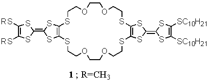
We designed the TTF-bisannulated molecule 1, which has
both the electrically active TTF units and macrocyclic moiety of
ion-recognition ability. We have found that the F4TCNQ
complex of molecule 1 forms nanowire structures, which
grows on mica recognizing K+ array of six-fold
symmetry.
- T. Nakamura, Handbook of Organic Conductive Molecules
and Polymers pp.727-780, H. S. Nalwa (ed.), vol. 1,
John Wiley & Sons, Chichester (1997).
- T. Akutagawa, T. Ohta, T. Hasegawa, T. Nakamura, C. A.
Christensen and J. Becher, Proc. Natl. Acad. Sci. USA,
99, 5028-5033 (2002).
THEORY OF AN ALL-CARBON MOLECULAR SWITCH: FULLERENES
BETWEEN NANOTUBE ELECTRODES
R. GUTIERREZ, 1 G. FAGAS, 2 R.
SCHMIDT, 1 and K. RICHTER 2
1 Institute for Theoretical Physics, Technical
University of Dresden, D-01062 Dresden, Germany
2 Institute for Theoretical Physics, University of Regensburg,
D-93040 Regensburg,Germany
We have recently shown in model calculations that
geometry-induced interfacial effects on electron transport across
molecular junctions are greatly enhanced in the presence of
mesoscopic electrodes [1]. In particular, for molecules between
carbon nanotube electrodes, which support low-dimensional
transport and share a rich topology, the conductance depends
crucially on the exact atomic configuration at the interface.
This owes to the importance of quantum intereference at the
molecular scale [2].
Here, we first give an overview of our studies on electron
transport across a carbon molecular junction consisting of a C60
molecule sandwiched between two semi-in�nite metallic carbon
nanotubes [3]. Within a tight-binding approach parametrised by
density functional theory, it is shown that the Landauer
conductance of this carbon hybrid system can be tuned within
orders of magnitude not only by varying the tube-C60
distance, but more importantly at fixed distances by either i)
changing the orientation of the Buckminsterfullerene or ii)
rotating one of the tubes around its cylinder axis. Furthermore,
it is explicitely shown that structural relaxation determines
qualitatively the transmission spectrum of such devices and a
detailed account of the parameters which control the conductance
is given. Finally, we focus on the contribution of additional
states appearing within the HOMO-LUMO gap of an isolated C60
molecule, which are attributed to the specifics of the molecular
junction and lie in the vicinity of the equilibrium Fermi energy
[4]. This contrasts the general view that electron transport
takes place in a resonant tunneling fashion via the molecular
orbitals, and reveals an analogy to the metal-induced gap states
(MIGS) at a metal-semiconductor-metal junction. We also show that
for carbon nanotube electrodes terminated by polyhedral caps the
conductance is dominated by the presence of such states and may
be efficiently controlled by applying a gate potential to the
fullerene.
[1] G. Fagas, G. Cuniberti, and K. Richter, Phys. Rev. B 63,
045216 (2001).
[2] G. Cuniberti, G. Fagas, and K. Richter, to be published in
Chem. Phys. (2002).
[3] R. Gutierrez, G. Fagas, G. Cuniberti, F. Grossmann, R.
Schmidt, and K. Richter, Phys. Rev. B 65, 113410 (2002)
[4] R. Gutierrez, G. Fagas, R. Schmidt, and K. Richter, in
preparation
TRAPS FOR CHARGE CARRIERS IN MOLECULAR MATERIALS FORMED BY
DIPOLAR SPECIES: TOWARDS LIGHT-DRIVEN MOLECULAR SWITCH
J. SWORAKOWSKIa, S. NEŠPŮrEKb
aInstitute of Physical and Theoretical Chemistry,
Wroclaw University of Technology, Wyb. Wyspianskiego 27,
PL-50-370 Wroclaw 51, Poland. E-mail:
sworakowski@pwr.wroc.pl
bInstitute of Macromolecular Chemistry, Academy of
Sciences of the Czech Republic, Heyrovského nám. 2, CZ-162 06
Praha 6, Czech Republic. E-mail:
nespurek@imc.cas.cz
Earlier work of the present authors [1-5] demonstrated that
the presence of polar species in molecular materials should
result in creation of traps for charge carriers localised on
neighbouring molecules, their depths and cross sections depending
on the dipole moment of the polar guest molecule. Based on the
concept of ‘dipolar traps’, a scheme of a light-driven
current switch is put forward. The switch would consist of a
molecular wire (e.g., a conjugated polymer chain) with suitably
chosen photochromic moieties placed in its vicinity or chemically
attached to the main chain. A reversible photochemical reaction
occurring in the photochromic species should reversibly change
their dipole moment resulting in creation of trapping sites on
the chain.
The architecture of the light-driven molecular switch and
basic requirements for its segments will be discussed. In
particular, the competition between dipolar and chemical trapping
will be considered.
[1] J. Sworakowski and S. Nešpůrek,
Polish J. Chem. 72 (1998) 163.
[2] J. Sworakowski, IEEE Trans. Diel. Electr. Insul. 7 (2000)
531.
[3] S. Nešpůrek, J.
Sworakowski, A. Kadashchuk, IEEE Trans. Diel. Electr. Insul. 8
(2001) 432.
[4] S. Nešpůrek, J.
Sworakowski, Thin Solid Films 393 (2001) 168.
[5] J. Sworakowski, S. Nešpůrek,
in: Molecular Low Dimensional and Nanostructured Materials for
Advanced Applications. (Eds. A. Graja, V. M. Agranovich, F.
Kajzar), NATO ASI Series, Kluwer Acad. Publ., Dordrecht 2002, in
press.
Charge transfer processes and environmental degreEs of
freedom: cooperativity and non-linearity
ANNA PAINELLI, FRANCESCA TERENZIANI
Dipartimento di Chimica GIAF, Università
di Parma,
viale delle Scienze 17/A, 43100 Parma, Italy; INSTM UdR Parma
The charge- (or electron-) transfer is at the heart of the
behavior of molecular materials for advanced applications.
Understanding the subtle interplay between electrons and
environmental degrees of freedom (including vibrations) is
fundamental to understand and fully exploit the interesting
properties of these materials. Here we concentrate on a
paradigmatic class of materials: donor-acceptor (DA) conjugated
chromophores.
In DA chromophores the intermolecular charge-transfer state is
responsible for strong absorption bands in the visible region,
whose large dependence on the polarity of the environment is
known since date. This same state is also responsible for the
large NLO responses of these molecules, and dominates their
linear and non-linear spectral properties. Within a two-state
picture for the electronic problem, we demonstrate a large
amplification of the non-linearity of the electronic system as
due to the interaction with slow degrees of freedom. The
spectroscopic signatures of this amplified non-linearity are
shortly discussed with reference to experimental data on DA
chromophores in solution.
In dense samples, including e.g. crystals, (poled) films,
functionalized polymers, or Langmuir Blodgett films,
inter-chromophore interactions are an additional source of
non-linearity. Each chromophore in fact feels the electric field
generated by the surrounding chromophores and then readjusts its
polarity, leading to a variation of the environmental field.
Adding intermolecular electrostatic interactions to the two-state
model for the isolated chromophore, leads to an interesting model
for interacting polar and polarizable chromophores. By varying
the relative chromophore orientation and/or the strength of
electrostatic interactions, the system is easily driven from a
neutral (N) ground state towards an ionic (I) ground state,
dominated by the zwitterionic form. The charge-transfer process
is localized within each chromophore, but the N-I transition we
observe in our model shares the same physics as the N-I
transition observed in mixed-stack charge-transfer salts, where
the charge-transfer interaction is delocalized along the chain.
Inter-chromophore interactions not only affect ground state
properties, but also show up in spectral properties with exotic
excitonic effects.
CORRELATIONS BETWEEN LARGE POLARONS IN MOLECULAR
CHAINS
L. BRIZHIK, A. EREMKO
Bogolyubov Institute for Theoretical Physics , Ukrainian
National Academy of Sciences, Metrologichna Str., 14-b, 03150
Kyiv, Ukraine
The self-trapped (spontaneously localised) electron states in
one-dimensional molecular chains are studied with account of
electron correlation. It is shown that the autolocalized states
of a few extra electrons in a deformable chain are described
within the zero adiabatic approximation by the many-component
nonlinear Schroedinger equations.
It is proved that in the case of two extra electrons the
minimum of total energy of the system corresponds to the singlet
bipolaron (bisoliton) state, which describes bound state of
electrons localised in a single potential well, created by the
self consistent chain deformation. In the same zero adiabatic
approximation, two electrons in the triplet state form two almost
free solitons (large polarons), localised in distant potential
wells. Between such solitons the repulsion exists, that decreases
exponentially with distance between the solitons centre of mass
coordinates. It is shown that the account of nonadiabatic terms
in the Hamiltonian results in the attraction between polarons via
virtual phonon exchange. In the result, the two-soliton state is
created, which is described by the double-hump localised
function. The equilibrium distance between function maxima is
determined both by the adiabatic and nonadiabatic terms of the
Hamiltonian. This stabilisation occurs due to the competition
between Pauli repulsion and the mutual attraction of polarons
arising from electron-phonon interaction.
Similarly, four electrons bind into two bound bisolitons with
the finite distance between them. As a result of electron
correlation, arising from the Pauli principle and electron-phonon
interaction, at zero temperature Ne extra electrons in
a chain create the periodic lattice of bisolitons in the form of
the Froehlich charge density wave.
THERMOLUMINESCENCE OF ORGANIC MATERIALS FOR OPTO-ELECTRONIC
APPLICATIONS
J. ULANSKI, I. GLOWACKI, E. DOBRUCHOWSKA, B. LUSZCZYNSKA
Department of Molecular Physics, Technical University of Lodz,
Zeromskiego Str. 116, 90-924 Lodz, Poland
Thermoluminescence (TL) was developed as a method of
investigation of charge carrier trapping, and up to now it is
regarded as one of the most direct methods for characterisation
of trapping sites. In this work we demonstrate, that this
technique yields also an insight into other phenomena, important
for performance of opto-electronic devices.
We analyse our TL investigations for a broad range of organic
materials, which can be used as components in various
opto-electronic applications: photovoltaic cells, LED or FET.
Both non-conjugated polymers, like poly(N-vinylcarbazole)
and its derivatives, or N-carbazolyl substituted silane
homo- and copolymers, and also -conjugated
polymers, like various poly(arylenevinylene)s, polyfluorenes and
poly(para-phenylene)s, as well as p- and n-type
discotic liquid crystals were investigated.
It is shown, that detailed analysis of TL (by means of
partial-heating technique and spectral analysis of emitted
light), performed in a broad temperature range (from LH2
temperatures range) and combined with other techniques, like
thermally stimulated currents, photo-discharge,
photoluminescence, electroluminescence and dielectric
spectroscopy, may allow to determine the mechanisms of: charge
carrier recombination; nature of undesired, long-wavelength
emitting sites; relationship between charge carrier trapping and
polymer morphology and molecular relaxations (‘wet-dog’
effect); or photo- and thermal degradations.
COMPARATIVE THERMOLUMINESCENT STUDY OF p - AND s
-CONJUGATED POLYMERS
A. KADASHCHUKa, H. BÄSSLERb, S. NEŠPŮREKc
aInstitute of Physics, National Academy of Sciences
of Ukraine, Prospect Nauki 46, 03028 Kiev, Ukraine, e-mail:
kadash@iop.kiev.ua
bPhilipps-Universität Marburg,
Hans-Meerwein-Strasse, D35032 Marburg, Germany
cInstitute of Macromolecular Chemistry, Academy of
Sciences of the Czech Republic, Heyrovsky Sq.2, 16206 Prague 6,
Czech Republic
The charge-carrier transport in both p
- and s - conjugated polymers has been
believed to be controlled by charge hopping through intrinsic
states derived from domainlike segments of the main chain. There
are certain indications that extrinsic traps could also play an
important role in these polymers, however the nature of trapping
states is still unclear. It was recently showed that thermally
stimulated luminescence (TSL) could be an efficient tool for
studying localized states and their energy distribution in
disordered semiconducting polymers. In the present work we report
on comparative TSL study of selected p
-conjugated polymers, as methyl-substituted ladder-type
poly(para-phenylene) (MeLPPP) and different PPV derivatives, and
some s - conjugated polysilanes.
The obtained TSL data for p
-conjugated polymers are interpreted in terms of recently
developed model of thermally assisted hopping in disordered
material, which allows quantitative evaluation of the
distribution of localized states for charge carriers. In
particular, we found that the distribution of localized states
for charge carriers in a series of substituted PPVs can be
described by a double-peak Gaussian DOS function. The shallower
peak is due to the inhomogeneously broadened distribution of
intrinsic hopping sites while the deeper one can be ascribed to
extrinsic traps which are most probably of ”aggregate” origin
and inherent for PPV-type polymers implying that charge transport
is also affected by such traps.
TSL results for studied s
-conjugated polysilanes suggest importance of polaronic effects
in these polymers. A model of low-temperature energy relaxation
of polarons in a disordered hopping system was formulated. The
model proves that the relaxation of polarons is much slower than
that of charge carriers in similarly disordered but rigid hopping
system and explains observed characteristic features of TSL in
polysilanes.
SPECTROSCOPIC STUDIES OF CHARGE-ORDERING SYSTEM IN ORGANIC
CONDUCTORS
K. YAKUSHIa, K. YAMAMOTOa, R. SWIETLIKa,
R. WOJCIECHOWSKIa, K. SUZUKIa, T. KAWAMOTOb,
and T. MORIb , Y. MISAKIc, K. TANAKAc
aInstitute for Molecular Science, Nishigo-naka,
Myodaiji, Okazaki, 444-8585, Japan
b Department of Organic and Polymeric Materials,
Tokyo Institute of Technology, 2-12-1, O-okayama, Meguro-ku,
Tokyo 152-8552 Japan
cDeparment of Molecular Engineering, Kyoto
University, Yoshida-Honmachi, Sakyo-ku, Kyoto 606-8501 Japan
In molecular conductors, the molecular orbital barely overlap
with those of neighbor molecules. Owing to this very small
overlap integral, the molecular conductors are located at the
boundary between a metal (delocalized state) and insulator
(localized state). When the charge is localized, the charge often
induces a charge disproportionation and eventually produces a
inhomogeneous charge distribution. This localized state is called
as a charge-ordered (CO) state, since the localized charges form
a new periodic structure.
Recently, metal-insulator phase transitions accompanied by
such CO are found in several organic conductors. We are
investigating the CO phase transition by using C=C stretching
modes as probes of the charge distribution. The authors have
reported the phase transitions in -(BDT-TTP)2Cu(NCS)21)
and -(ET)2RbZn(SCN)42)
by means of polarized reflection and Raman spectroscopy. Both
compounds exhibit drastic changes in the Raman spectra below the
CO phase transitions. The single Raman band splits into several
bands reflecing the lowering of symmetry accompanying the
localization of charge. In this manner, we have demonstrated that
the vibrational spectroscopy is a power tool to study the CO
phase transition. High pressure is an effective method to change
the electronic state of organic conductors, because they are
located at the boundary between a metal and insulator. Using a
high-pressure Raman spectroscopic method, we are investigating
organic CO systems such as -(ET)2TlZn(SCN)4,
-(ET)2IBr2, -(ET)2I3, and
(TTM-TTP)I3. We will present several recent results.
1) J. Ouyang, K. Yakushi, Y. Misaki, and K. Tanaka,
Phys. Rev. B, 63, 054301 (2001).
2) K. Yamamoto, K. Yakushi, K. Miyagawa, K. Kanoda,
and A. Kawamoto, Phys. Rev. B, 65, 085110 (2002).
ELECTRICAL AND SPECTRAL PROPERTIES OF ORGANIC SALTS FORMED
FROM BEDT-TTF AND MAGNETIC ANIONS
A. GRAJAa, A.
ŁAPIŃSKIa AND V.A. STARODUBb
aInstitute of
Molecular Physics, Polish Academy of Sciences, Smoluchowskiego
17, 60-179 Poznań, Poland, graja@ifmpan.poznan.pl
bDepartment of Chemistry, Kharkov National Karazin
University, 61077 Kharkov, Ukraine,
vladimir.a.starodub@univer.kharkov.ua
Structural dimensionality, and thus the electronic
dimensionality, is of great importance for the physical
properties of low-dimensional molecular solids. Recently, much
attention being devoted to the exploration of the novel lattice
architectures and physical properties resulting from the
association of organic cation radicals (e.g.
bis(ethylenedithio)tetrathiafulvalene, BEDT-TTF) with bulky
anions (e.g. polyoxometalates). One of the reasons for the
interest in polyoxometalate-based materials, containing both
localized and delocalized electrons is the possibility of
creating compounds where the coexistence of co-operative magnetic
and electrical properties such as ferromagnetism and
superconductivity can be observed.
A structure of these hybrid material is usually built of
alternating organic and inorganic layers. The organic layers are
created by peculiar arrangement of BEDT-TTF species with short
intermolecular contacts. The inorganic ones are formed of
polyoxometalate anions and solvent molecules. Both, organic and
inorganic building blocks show a structural disorder which is so
important for the electron distribution in these blocks.
Structural, electrical and spectral properties of two
organic/inorganic hybrid crystals are presented and discussed.
The new organic CT salt (BEDT-TTF)6(Mo8O26)(DMF)3,
where DMF is a dimethyl formamide, is characterised. It exhibits
metallic properties with anomalies at about 180 and 60 K. The
anomaly at 180 K, confirmed by IR spectral investigation, is
caused by changes in a charge carriers scattering mechanism
(domination of electron-phonon scattering for T > 180 K, and
electron-electron scattering for T < 180 K). The distinct
anomaly at 60 K, not observed by spectral methods, could be
explained by spin transition and/or rearrangements of organic and
inorganic sublattices. IR and Raman spectra of single crystals
are analysed and an assignment of the vibrational features is
proposed. The T-dependencies of the transport parameters are
obtained using the Drude - Lorenz model. For comparison, the
spectral properties of the hybrid semiconducting salt (BEDT-TTF)2(W6O19)
are also presented and discussed.
CALCULATIONS OF NONLINEAR OPTICAL PROPERTIES
OF ORGANIC STRUCTURES
V.M. YARTSEV
Centro de Física, Instituto Venezolano de Investigaciones
Científicas (IVIC),
Apartado 21827, Caracas 1020-A, Venezuela; e-mail:
syartsev@ivic.ve
Organic structures present fascinating prospects of
customer-adapted practical applications due to their ability to
be modified on the molecular level in a very precise and subtle
way. Our recent work [1-6] on modeling organic structures will be
evaluated with respect to understanding relative significance of
the following factors: size, chemical composition, configuration,
dimensionality, symmetry, electronic correlation, electron
coupling to internal vibrations. The molecular dimer is a very
convenient system for investigation of the electronic
correlation: the model is simple enough to allow (in several
important limiting cases) analytical relations for the first and
second hyperpolarizabilities as a function of the transfer
integral, Hubbard on-site repulsion energy, and small polaron
binding energies. However, this model cannot account for changes
in the molecular configuration which may be made either
permanently by an appropriate chemical synthesis or induced by an
external light irradiation. In this case, the model of four sites
is working well: two sites describe the central part (bridge) and
the other two the attached electroactive groups which may have
different angles with respect to the bridge. Other parameters
include donor and/or acceptor abilities of the side groups,
intersite transfer integrals, bridge length, intrasite
flexibility. These parameters have a clear physical meaning, can
be estimated independently, and may be modified in a controlled
way by an appropriate molecular engineering. Hyperpolarizability
tensors are calculated and the results suggest what kind of
changes in geometry are needed for optimization of specific
components. The role of interaction between organic molecules in
adjacent layers in the Langmuir-Blodgett films is also discussed.
Taken together, modeling of organic structures by a set of
interacting sites offers a relatively simple way to obtain a
theoretical design of molecular structures with high nonlinear
optical properties.
[1] V.M. Yartsev, Chem. Phys. Lett. 313, 241
(1999).
[2] V.M. Yartsev, A. Marcano, Synth. Metals 115,
197 (2000).
[3] V.M. Yartsev, Nonlin. Optics 26, 107 (2000).
[4] V.M. Yartsev, A. Marcano O., Rev. Mex. Fis. 47
(S.1), 48 (2001).
[5] V.M. Yartsev, M.R. Singh, Synth. Metals 127,
115 (2002).
[6] V.M. Yartsev, M.R. Singh, Chem. Phys. 276,
293 (2002).
The lipid bilayer principle: From Soap bubbles to black
lipid membranes (BLMs) to biosensor Applications
H.Ti. Tien, Angelica Ottova
Department of Physiology, Biomedical and Physical Sciences
Building, Michigan State University, East Lansing, MI Michigan
48824
In the past decade there have been a number of reports on self
assembled molecules or structures as 'advanced materials' or
'smart sensors' [1]. Without question, the inspirations for these
exciting findings come from the biological world, where, the
lipid bilayer of cell membranes plays a pivotal role. Self
assembled bilayer lipid membranes (BLMs or planar lipid bilayers)
on solid or gel supports may be formed by a number of methods
[2]. A,s an example, it has been demonstrated that by doping an
s-BLM or sb-BLM with fullerenes such as C60, it is possible to
construct sensor probes, and to investigate redox reactions and
light induced electron transfer across the lipid bilayer. The
C60-containing s-BLM or sb-BLM, considered basically as a
'molecular device', is a light sensitive diode that is capable of
photoinduced charge separation that undergoes redox reactions
across the substrate/hydrophobic lipid bilayer/aqueous solution
junctions. Using cyclic voltammetry, our results show that C60
embedded in the BLM can act as an excellent electron carrier or
mediator and should be useful for electrochemical biosensor and
molecular electronics device development. Supported BLMs,
possessing the structural and dynamic properties of conventional
planar lipid bilayers, are excellent models for investigating
basic membrane-mediated ligand-receptor contact interactions [2].
They are ideal systems for incorporating a host of compounds
including fullerenes, semiconducting rianoparticles, receptor
proteins, and polymeric materials for practical applications [3].
References
- H. T. Tien and A. L. Ottova, Membrane Biophysics:as
viewed from experimental bilayer lipid membranes (planar
lipid bilayers and spherical liposomes), Elsevier
Science, Amsterdam, the Netherlands, 2000 .
- H. T. Tien and A. Ottova "The Lipid Bilayer Concept
and Its Experimenta.l Realization: From Soap Bubbles, the
Kitchen Sink, to Bilayer Lipid Membranes", J.
Membrane Science, 189 (2001) 83
- Ottova and H. T. Tien, The 40th anniversary of bilayer
lipid membrane research, Bioelectrochemistry. 56, (2002)
NOVEL ELECTRICAL AND OPTICAL PROPERTIES OF CONJUGATED
MOLECULES AND POLYMERS DEPENDENT ON MOLECULAR STRUCTURES AND
NANOSCALE STRUCTURES.
EFFECTS OF NANOSCALE PERIODIC STRUCTURE-
K. YOSHINO, H. TAKEDA, M. KASANO, N. TAKAMOTO, T. UMEDA, Y.
YOSHIDA, T. MATSUI, Y. NISHIHARA, A. FUJII, M. OZAKI
Department of Electronic Engineering, Graduate School of
Engineering, Osaka University
2-1 Yamada-oka, Suita, Osaka 565-0871, Japan
Novel electrical and optical properties of conjugated
molecules and polymers with various molecular structures in
nano-scale periodic structures are studied in details.
Nano-scale periodic structures of the conjugated polymers and
carbons as 3-dimensional photonic crystals were prepared by
infiltrating the conjugated polymers and carbons in the
interconnected nano-scale voids in synthetic opals and inverse
opals of the conjugated polymers and carbons made by removing
silica from infiltrated opals by HF.
These infiltrated opals and inverse opals made of the
conjugated polymers and molecules exhibited the novel electrical
and optical properties such as unique tunable optical reflection
and transmission spectra, unique gel like behavior and lasing
upon optical excitation.
Nano-scale periodic structures of conjugated polymers and
molecules were also prepared by irradiation interfering optical
beam on the surface of the polymer film having azo-chromophore in
the structures and also doped with the conjugated polymers or
molecules. Their surface relief structures can be interpreted to
be a two-dimensional photonic crystals and various novel optical
properties have been observed.
Cholesteric liquid crystals and ferroelectric smectic liquid
crystals doped with conjugated molecules exhibits the
characteristics as one-dimensional photonic crystals and even
tunable lasing was observed in these systems.
To understand their characteristics photonic band schemes have
been theoretically calculated and various new effects were
demonstrated.
ORGANIC MEDIA FOR 3-D OPTICAL MEMORY: MODERN TRENDS
V.BARACHEVSKY
Photochemistry Center, Russian Academy of Sciences, 7a,
Novatorov Street, Moscow, 117421, Russia
barva@photonics.ru
Using literature and own data the state of the art and future
for making light - sensitive recording organic media which are
suitable for 3-dimensional archive and working optical memory are
analyzed. At present these media have aroused considerable
interest in connection with the intensive development of
telecommunication networks and Data Bases with super high
information capacity.
The analysis shows that dry photopolymerizable materials
containing photobleaching dyes as photoinitiators for
polymerization provide registration of deep hologram with a high
diffraction efficiency and thus a high angle selectivity during
registration and read-out holograms. Application of two-photon
polymerization and irreversible photochemical transformations of
organic compounds is acceptable for bitwise 3-D optical memory
too. In this case read-out of optical information is achieved by
use of photoinduced refraction or luminescence.
On the development of recording media for working 3-D optical
memory photochromic materials are best suited to application.
These media provide bitwise registration of optical information
as a result of reversible transformation of organic compounds
exhibiting photoinduced refraction or luminescence too.
At last, the possibility for realization bitwise frequency -
selective 3-D optical memory based on processes of photoinduced
aggregation - deaggregation as well photochemical burning organic
compounds is discussed
Achieved results in the above mentioned science lines are
illustrated by certain examples.
ROUGH ELECTRODE SURFACE: EFFECT ON CHARGE CARRIER INJECTION
AND TRANSPORT IN ORGANIC DEVICES
S.V. NOVIKOV
A.N. Frumkin Institute of Electrochemistry, Leninsky prosp.
31, 119071 Moscow,
Russia, email: vanlab@online.ru
Effect of electrode roughness on charge carrier injection and
transport is considered. Explicit formula connecting roughness
profile of an electrode with the distribution of the electric
field at its surface (and electrostatic potential in the bulk of
transport layer) is derived for the case of smooth roughness,
when typical height of roughness element is small in comparison
to its size across a surface (this is a very typical situation).
This formula gives us a possibility to measure the electrode
surface profile (e.g., by AFM) and then calculate various
injection properties of this particular electrode for any kind of
injection rate (e.g., Fowler-Nordheim or Schottky-Richardson):
total injection current, surface distribution of injection peaks
etc. Smooth roughness leads to relatively small spatial
fluctuation of electric field at the surface, yet because of
highly nonlinear relation between electric field and injection
current even these small fluctuations may result in giant
fluctuation of the current. In some cases effect of smooth
roughness is so strong that the functional dependence of the
total injection current on electric field is completely changed.
For this reason, calculation of injection parameters from the
injection current data, carried out without respect of the
electrode roughness, may produce wrong numbers. General
properties of electrode - organic layer interface in the case of
significant (not smooth) roughness are considered and a suitable
numeric procedure for the calculation of the surface electric
field distribution is suggested. It is shown also that rough
surface of electrodes generates an additional energy disorder in
the bulk of transport layer. This principal result indicates that
electrode roughness affects not only carrier injection but
carrier transport as well. Magnitude of the disorder is
proportional to voltage applied to the device and decays as
inverse distance to the electrode for distances much greater than
surface correlation length. Roughness-induced energetic disorder
produces a channel-like structure in the vicinity of the
electrode (typical scale being the surface correlation length,
50-100 nm in many cases), thus providing the separation of
electrons and holes. Such separation should decrease charge
recombination rate and, hence, emitting efficiency of light
emitting devices. At the same time, the separation is favorable
for solar cells. Implications of electrode roughness on optimal
design of devices are considered.
ELECTRICAL VS STRUCTURAL AND MECHANICAL PROPERTIES OF
POLYANILINE-BASED CONDUCTING SYSTEMS
P. Fedorko, J. Fraysse, J. Planes, D. Djurado, B. Dufour, P.
Rannou, A. Pron, J.P. Travers
Laboratoire de Physique des Métaux Synthétiques, UMR 5819
(CEA-CNRS-UJF), DRFMC, CEA-Grenoble, France
In recent years, several routes have been investigated with
the goal of obtaining processible conducting polymers showing
both high electrical (quasi-metallic) conductivity and good
mechanical properties. In the case of polyaniline, one can cite:
i) the use of tailor-made protonating agents which combine doping
and plasticizing properties (internal plasticizers), ii) the
addition of an external plasticizer during the processing of
doped polyaniline, i.e. molecules which do not dope polyaniline
but only plasticizes it, and iii) the preparation of polyaniline
blends with classical insulating polymer matrix. We will present
and discuss the results of transport, structural and mechanical
studies in a series of materials belonging to the three
categories.
Using molecular engeneering concepts we synthesized series of
plasticizing dopants for polyaniline. Films cast from solutions
of doped polyaniline exhibit both high quasi-metallic
conductivity, and an excellent flexibility. As an example, films
with an elongation at break l/l0
» 200% were obtained. These films are
semicristalline. Nanocristallites present a lamellar structure
with an alternance of polyaniline chain and dopant layers.
The addition of external plasticizers induces dramatic changes
in the transport properties. First, the room temperature
conductivity increases significantly with increasing amount of
plasticizer whereas the relative proportion of conducting chains
in the material decreases. Second, we show for the first time
that a veritable insulator-metal transition (IMT) is induced by
the addition of plasticizers, leading to polymers which present a
finite conductivity at T= 0. However, mechanical properties are
only slightly improved.
Finally, blends of polyaniline with classical insulating
polymers are well known for presenting an extremely low
percolation threshold (<0.1 wt % of polyaniline). In this
case, one tries to maximize the conductivity while avoiding a
loss in the mechanical properties of the matrix. As a matter of
fact, in polyaniline / PMMA blends, some kind of ”mechanical
percolation” is observed for a polyaniline content higher than
that corresponding to the electrical percolation threshold. Above
the percolation, the polyaniline network appears as a mechanical
reinforcement of the matrix. The scaling law of percolation has
been checked as a function of temperature. While the percolation
threshold remains constant, a continous increase of the critical
exponent is observed. We propose a unique model, based on the
continuous percolation theory which accounts for the whole set of
data.
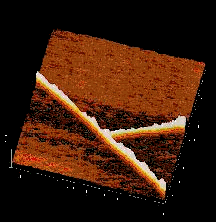
Deformation-Induced Molecular Alignment in Pentacene Thin
Films Characterized by Electron Microscopy and Diffraction
Lawrence F. Drummy, Paul K. Miska and David C. Martin
Department of Materials Science&Engineering, University of
Michigan, 2300 Hayward Street, Ann Arbor, Michigan MI 48109-2136
Pentacene is a material of current interest as the
semiconducting layer in all-plastic thin film electronic devices.
We have investigated the plastic deformation and resulting
molecular alignment of scratched and rubbed polycrystalline
pentacene thin films using optical and electron microscopy and
electron diffraction.
Polycrystalline films of pentacene were produced by vacuum
sublimation onto amorphous carbon coated substrates in a glass
tube, and the films had grain sizes of 500-5000 nm. Before
deformation the films are textured with the (001) planes
parallel to the substrate and the long axis of the molecules
nearly perpendicular to the substrate.
Inside the plastically deformed zone near the scratch, the
molecules lie down with their long axis parallel to the
substrate, and they are oriented in the scratch direction. We
used electron diffraction and high resolution electron
microscopy to quantify the extent of alignment in the deformed
region and to directly image defects visible after alignment.
The grain size of the film is reduced after deformation.
Outside the scratched zone the films are uniform on a
sub-micron length scale with density fluctuations in the form of
grain boundaries and holes on a length scale greater than one
micron. Inside the scratched zone the films are uniformly dense
on a length scale greater than one micron with density
fluctuations in the form of grain boundaries on a
nanocrystalline length scale.
DESIGN OF MOLECULAR MAGNETS
J.V. YAKHMI
Technical Physics and Prototype Engineering Division, Bhabha
Atomic Research Centre, Mumbai (Bombay) – 400 085, India.
(E-mail: Yakhmi@magnum.barc.ernet.in)
The conventional magnetic materials used in present-day
technology, such as, Fe, Fe2O3, Cr2O3,
SmCo5, NdFe14B etc. are all atom-based,
whose synthesis requires high temperature routes. Employing
ambient temperature synthetic organic chemistry, it has recently
become possible to engineer a bulk molecular material with
designer characteristics, including magnets. One essentially
makes use of the weak nature of intermolecular interactions in a
molecular solid, which lets the molecules retain their
individuality, making it possible to derive the properties of a
molecular solid from those of the molecular sub-units. Typical
synthetic approach to design molecule-based magnets consists of
choosing molecular precursors, each bearing an unpaired spin, and
assembling them in such a way that there is no compensation of
spins at the scale of the crystal lattice. Magnetism being a
co-operative effect, the spin-spin interaction must extend to all
the three dimensions, either through space or through bond.
Specific occurrence of ‘spin delocalisation’ and ‘spin
polarisation’ in molecular lattices is helpful in bringing
about ferromagnetic interaction by facilitating necessary
intermolecular exchange interactions.
Since the first successful synthesis of molecular magnets in
1986, a variety of them have been synthesized, which can be
classified on the basis of the chemical nature of the magnetic
units involved: organic-, metal-based systems, or mixed
organic-inorganic systems. A number of molecular magnets have
been assembled, through polymerisation process using
ferrimagnetic chains employing heterobimetallic species, in which
two different spin carriers are bridged by extended bisbidentate
ligands such as oxamato, oxamido, or oxalato, etc.
Apart from the fact that a molecule is the ultimate unit for
data-storage, the design of molecular magnets has also opened the
doors for the unique possibility of designing poly-functional
molecular materials, such as magnets exhibiting second-order
optical nonlinearity, liquid crystalline magnets, or chiral
magnets. Solubility of molecular magnets, their low density and
biocompatibility are attractive features. Being weakly colored,
unlike the opaque classical magnets, possibilities of
photomagnetic switching can be envisaged. Persistent efforts
continue to design the ever-elusive polymer magnets which when
made would have a huge impact on applications in industry.
This talk will highlight some recent developments in the field
of molecular magnetism, with some examples from the author’s
own lab.
Acknowledgements. This talk is dedicated to the memory
of the late Prof. Olivier Kahn, a pioneer in the area of
molecular magnetism, and a great source of inspiration.
DESIGN, SYNTHESIS, AND CHARACTERIZATION OF CATIONIC
WATER-SOLUBLE CONJUGATED POLYMERS
B. LIU1, Q.-L. FAN1, S. LU1,
W.-L. YU1, S.-J. CHUA1, W. HUANG1,2
1 Institute of Materials Research and Engineering,
National University of Singapore, 3 Research Link, Singapore
117602, Republic of Singapore
2 Department of Chemical and Environmental
Engineering, National University of Singapore, 10 Kent Ridge
Crescent, Singapore 119260, Republic of Singapore.
chehw@nus.edu.sg
In this talk, we report our recent studies on the design,
synthesis, and characterization of novel cationic water-soluble
conjugated polymers. Through the functionallization of
polyfluorene (PF) and poly(p-phenylene vinylene) (PPV)
derivatives with amino-terminal groups, cationic water-soluble
polymers with different color emissions have been achieved, with
the water-solubility realized through the post-polymerization
method, which permits the full structural characterization and
the control of the cationic degree. Herein the PPV derivatives
present the first examples of the cationic water-soluble
polymers, which emit red and green light. It was demonstrated
that the ionization of the side chains reduced the effective
conjugation of the backbones of the polymers. The complexation of
PPV-NEt3Br with the oppositely charged polyanions,
such as PAANa, in aqueous solution induces the PPV chain to vary
from isolated state to aggregated state and then to be surrounded
by PAANa chains with increasing amount of PAANa. The complexation
dependent spectral change provides a strategy for studying
complexation behavior between oppositely charged polymers and has
potential applications in sensory technologies.
Breakthroughs have also been achieved in the synthesis of blue
emission conjugated polymers with tunable water-solubility, which
provide enriched materials for the self-assembly study. It was
also found that the neutral polymers had good solubility in water
upon the addition of some weak organic acids. Instead of forming
the quaternized salt, only weak interaction exists between the
acid and the amino-terminal groups. Detailed characterization
results have shown good thermal stability and reversible
electrochemical properties for both the neutral and the
water-soluble polymers. The special solubility and intense
fluorescence both in solutions and as films endow this series of
materials most attractive candidates as the transporting/emitting
layer in the multi-layer device fabrication.
Giant Optical Rotatory Power and Light Modulation
Properties in Biodegradation of Poly(Lactic Acid) Films
Y. TAJITSU
Department of Polymer Science & Engineering, Yamagata
University
Yonezawa, Yamagata 992-8510, JAPAN
e-mail: tajitsu@yz.yamagata-u.ac.jp, FAX: 81-238-26-3410
Every year, the amount of industrial waste is increasing, and
as a result, environmental pollution has become more serious than
ever. As a material that is expected to solve environmental
pollution, biodegradable polymers have attracted much attention.
Polylactic acid (PLA) is one polymer material on which
biodegradability research has been most advanced. PLA is a chiral
polymer in which molecules containing asymmetric carbon atoms
have a helical orientation. Two optical isomers exist in PLA. One
is PLLA, and the other is PDLA. For a long time, chiral polymers
have been expected to exhibit optical rotary power, , in their solid state, compared
with inorganic low-molecular-weight crystals. A typical substance
with a large is -quartz (-SiO2). The of
-quartz is due to the
helical structure formed by molecules. Therefore, it is believed
that of a chiral polymer is
large. However, no PLA film with a large
had been prepared to date, because it was very difficult to
control its higher order structure. In this study, we prepared
PLLA with a molecular weight Mw of 100,000 ~
600,000 and an isomer (D-type) content (ID) of 0.001 ~ 1.000%.
Then, using physical processes, we fabricated various samples
such as oriented PLLA film, PLLA fiber, rolled PLLA film and a
cylindrical plate. Finally, we observed a large and high-speed light modulation
(LM) in the cylindrical plate fabricated using a new physical
process. The findings for the cylindrical plates fabricated using
a new physical process are summarized as follows:
1) Existence of significantly large
in the fiber axis direction of PLA films
PLLA and PDLA films possess levorotatory power and
dextrorotatory power, respectively. The
of PLLA film is 7200˚/mm and approximately 300 times larger than
that of -quartz.
2) Demonstration of LM by PLLA films
We confirmed LM up to 10 MHz. We believe that the LM speed in
the GHz range of a highly modified PLLA sample fabricated using
the new physical process is possible because the PLLA film
provides a rapid response.
FEATURES OF CHARGE CARRIER CONCENTRATION
AND MOBILITY IN p
-CONJUGATED POLYMERS.
G.JUŠKAa,
K.GENEVIČIUSa, K.ARLAUSKASa, R.ÖSTERBACKAb,
H.STUBBb
a Department of Solid
State Electronics, Vilnius University, Saulėtekio 9, LT-2040
Vilnius, Lithuania gytis.juska@ff.vu.lt
b Åbo Academy University, Department of Physics,
Porthansgatan 3, FIN-20500
Turku, Finland rosterba@abo.fi
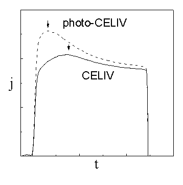
We will represent the experimental results of investigation of
photoexcited and of equilibrium charge carrier mobility and
concentration by charge carrier extraction by linearly increasing
voltage method (CELIV) in pi-conjugated polymers (PPV, RRPOT,
RRPHT, RRaPHT, etc.). From the numerical modelling and
experimental investigation by CELIV the nature of mobility
dependence on electric field can be estimated [1].
The following obtained experimental results will be discussed:
- the conductivity dependencies on temperature and electric
field are caused by drift mobility;
- the dependence of drift mobility on electric field is
caused by electric field induced release from trapping
states;
- in low electric field region the TOF mobility decrease
with increasing electric field is caused by the electric
field redistribution;
- the transients of mobility and concentration of
photoexcited charge carriers obtained from photo-CELIV
measurements (Fig.1).
 [1] G.Juška
et al. Phys.Rev. B62, R16235 (2000)
[1] G.Juška
et al. Phys.Rev. B62, R16235 (2000)
Fig.1. Schematic view of current transients of
CELIV and photo-CELIV.